


Invited Speakers
Nikolay Cherkashin
CNRS, CEMES, Toulouse
France
Nikolay Cherkashin obtained his PhD in Semiconductor Science in 2002 from the Ioffe Institute, Saint-Petersburg, Russia and Habilitation at University of Toulouse III, France in 2017. He is a senior scientist at CNRS, CEMES, Toulouse, France. He was the head of MEM group: Materials and devices for Electronics and Magnetism at CEMES. His interests range from the nanosystems like quantum dots and quantum wells to nano and micros-precipitates created during ion implantation, with focus on studies by means of transmission electron microscopy. He is an inventor of three TEM based techniques for strain and polarization quantification in crystalline materials, namely, Moiré by specimen design (“MoSD”), Absolute strain (“AbStrain”) and “Relative displacement”.
From Imaging to Quantification: Advanced TEM for Implantation-Induced Defects in Crystalline Materials
Ion implantation is a key process in modern microelectronics. Understanding the formation, evolution, and impact of implantation-induced defects is essential for device performance and advanced wafer engineering. Transmission electron microscopy (TEM) provides unique access to these defects across length scales, from sub-nanometer clusters to micrometer-sized extended structures. This talk will highlight selected advanced TEM-based techniques for the quantitative characterization of ion-implanted semiconductors.
Wolfgang Diewald
Infineon Technologies Austria AG
Austria
Wolfgang Diewald holds a PhD in chemistry and brings 30 years of experience in semiconductor technology at Infineon, working across various frontend sites. His expertise spans technology development, process integration, product engineering, high-volume manufacturing, unit process development, and equipment strategy. He currently serves as the Senior Vice President Technology in Infineon Technologies Austria AG.
Unit Processes as Technology Differentiators
Infineon is renowned for its exceptional semiconductor devices, built on differentiating technologies. Achieving this high level of performance requires both innovative integration concepts and cutting-edge unit processes. This lecture will provide insights into key unit processes that serve as enablers for unique technological advancements, illustrated through a series of examples.
Hiro Ito
Applied Materials Japan, Inc.
Japan
Dr. Hiro Ito received his BEng from Kyoto University, Japan, and his Ph.D. from the University of Salford, UK. Since 1989, he has been working at Applied Materials, focusing on the development of ion implanters and their applications.
Evolutional journey of ion implanters along device technology pathway
Ion implantation was first adopted to fabrication of micro devices in early 70s. Since then, the devices kept evolving in both performance and functions, which in turn brought strong needs to advance ion implanters to gain specific capabilities. The journey through the past half century has transformed the ion implanters from simple doping tool to universal material engineering system. This paper discusses the key milestones along the journey.
Roy Knechtel
Schmalkalden University of Applied Sciences
Germany
Roy Knechtel is since 2019 Professor for Autonomous Intelligent Sensors at Schmalkalden University of Applied Sciences / Germany. His research interests are about sensors principles, multi-sensor-integration and sensor applications with focus on the sensor and especially MEMS Technologies, including wafer bonding. Before following the call to become a professor he was from 1998 until 1999 with X-FAB MEMS Foundry Technologies Erfurt. Here he developed in different positions Wafer Bonding processes and MEMS technologies such as for pressure and inertial sensors and microphones. Roy Knechtel holds a PhD in Micro-System-technologies. He authored more than 100 publications and more than 10 patents.
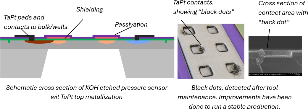
RTP Conditioning of Electrical Contacts in MEMS Pressure Sensors for Harsh Environmental Applications
Roy Knechtel1, Sophia Dempwolf2, Cora Preiß2, Lutz Ende2, Uwe Schwarz2
1Schmalkalden University of Applied Sciences, Germany; 2X-FAB MEMS Foundry GmbH Erfurt, Germany
MEMS pressure sensors, one of the oldest but most frequently used micro-system devices, are still acquiring new fields of application. One such field is harsh environments, such as high temperatures, exhaust or air conditioning or cooling systems with direct contact with related aggressive and corrosive media of which pressure needs to be measured for related control systems. While the silicon carrier and membrane of MEMS pressure sensors are chemically very stable, as are the related insulating layers made from thermally grown oxide, a special solution for electrical wiring metal, which is aluminium or aluminium alloys in standard applications, is needed. The solution here is to use a stack of tantalum as a barrier and adhesion layer instead of aluminium, and platinum and gold as corrosion-free metals for the signal lines in the sensors and at the bond pads to wire to the outer signal conditioning electronics (ASIC, PCB). This change in the metal system also affects the contact to the silicon, in which the piezo resistors acting as strain gauges are realised by ion implantation directly in the silicon. Here, a slight and well-defined alloying of the tantalum and in the complete stack is required, but without full diffusion, especially into the silicon of the piezo resistors. A certain diffusion is needed for low contact resistance, while too much diffusion would destroy the contacts. This special contact conditioning is realised by a rapid thermal process (RTP). The challenges and solutions concerning the interaction between the tantalum thickness and the RTP temperature as well as its control, especially with respect to achieving a stable production solution, will be described in this contribution.
Santosh K. Kurinec
Rochester Institute of Technology (RIT), New York
USA
Santosh K. Kurinec is a Professor of Electrical and Microelectronic Engineering at Rochester Institute of Technology (RIT). She is a Fellow of IEEE and a Member of the New York Academy of Sciences. She is a Guest Professor at Technical University of Applied Sciences Würzburg-Schweinfurt, Germany. She worked at IBM Watson Research Center as a visiting scholar. Her research activities include advanced integrated circuit materials & devices and photovoltaics. She is currently working on addressing energy consumption in semiconductor manufacturing and offsetting using renewables. She received the 2012 IEEE Technical Field Award for integrating research into teaching to prepare microelectronic engineers for future challenges. She was inducted in the Women in Technology International Hall of Fame in 2018. She received IEEE Region 1 William Terry Distinguished Service Award, 2022, for IEEE service, research and teaching. In 2024, she is appointed as Vice Chair of IEEE SRC Region 1-3, 7 and she is an IEEE EDS Distinguished Lecturer. She has over 140 publications in research journals and conference proceedings. She edited books on Energy Efficient Computing & Electronics: Devices to Systems, and Nanoscale Semiconductor Memories: Technology and Applications, and Emerging Photovoltaic Materials: Silicon & Beyond, and chapter on Ferroelectric Thin Films.
Energy and PFAS Chemical Consumption in Semiconductor Manufacturing
As microchips become more ubiquitous in modern technology, the semiconductor fabrication industry will keep growing to meet the demand for more complex and powerful devices. Semiconductor fabs use large amounts of energy. With this comes a heavy price on the global energy market, and a lesser-known price on environmental health and safety. Currently, most semiconductor manufacturing relies on traditional energy, particularly in regions where fossil fuels are the dominant energy source. As a result, an increasing number of studies have focused on integrating clean energy solutions and developing energy-efficient technologies to reduce the environmental impact of energy-related emissions within the sector. Major manufacturers are responding through green power purchases and RE100 commitments. On chemical side, many of the processes involved in semiconductor manufacturing use harmful chemicals and produce environmental and health-related toxins as waste. One group of these toxins are known as PFAS, or per- and polyfluoroalkyl substances. These are compounds that accumulate in the environment and organic tissues and are resistant to chemical breakdown, so they remain as toxins for long periods of time. A case study involving the energy usage for a standard metal-oxide semiconductor field-effect transistor (MOSFET) manufacturing process in a university semiconductor fabrication teaching laboratory will be presented. A prototype photovoltaic system is designed to offset the energy usage of this process providing a vision towards the use of renewables. For the chemical case study, a comparison of reactive ion etching to ion beam etching is done to observe differences in the efficiency and results of the processes and to compare their prospects for widespread use within industry. Reactive ion etching involves the use of harmful per- and polyfluoroalkyl (PFAS) substances. Ion beam etching is another etching technology that is less widespread in large-scale manufacturing but consumes inert gases and does not produce environmental toxins as a byproduct. The study of these two important areas, at an educational level, will be a way for the future of industry to improve the impact they have on society by re-engineering energy usage and re-thinking chemical usage.
Tetsuo Narita
Toyota Central R&D Labs., Inc. & Nagoya University
Japan
Tetsuo Narita, Ph.D., joined Toyota Central R&D Labs., Inc. as a senior researcher in 2007 and Nagoya University, Japan as a Visiting Professor since 2024. Dr. Narita specializes in process technologies involving epitaxial growth, ion implantation, and MOS gate structure, for III-nitride vertical power devices. He has published 116 peer-reviewed journal articles on semiconductor growth and analysis and served as Project Vice-Manager for the Consortium for GaN Research and Applications, Working Group on Crystal Growth.
Overview of Doping and Annealing for GaN Power Devices
For GaN as a III-V semiconductor, ion implantation can create both Ga and N vacancies, and its complexes, which plays as a role during post-implantation annealing. Mg ion implantation for p-type doping create N vacancies causing compensation, which can be reduced by the sequential N ion implantation. For the case of Si ion implantation for n-type doping, N vacancies can play as excess donors. We evidently show the suppression of excess donors by implanting O or N ions substituting anion sites.
Ashutosh Sagar
Implant, Anneal and Plasma surface treatment technologies, Intel
USA
Dr. Ashutosh Sagar is Principal Engineer and Director of Implant, Anneal and Plasma surface treatment technologies at Intel. During his more than 20 years of engineering innovations at Intel, he has lead the development and implementation of leading edge anneal and implant technology in Intel’s advanced nodes. In his talk, Dr. Ashutosh will discuss evolution of anneal and Implant technology to meet scaling demands of CMOS transistors. He will talk about the evolving need for overlap and synergy of anneal and implant technologies to keep pace with aggressive evolution of transistor architectures. Dr. Ashutosh has a PhD in Physics from Carnegie Mellon University.
Anneal Technology in CMOS manufacturing: Evolution and Synergy Opportunities with Implant
Transistor architecture evolution has driven aggressive demand for innovation in annealing technology. This talk will discuss examples of device requirements and how anneal technology has evolved to satisfy those requirements. In addition, Implant technology has also served device performance and material modification requirements. We will review use cases to make a case for anneal and Implant technology to further converge at a platform level and enable wider applications.
Woo Jin Seung
SK Hynix Inc. (Hyundai Electronics)
South Korea
Seung Woo Jin joined SK Hynix (Hyundai Electronics) on February 5, 1996. He has extensive experience in ion implantation and anneal processes, having served as team leader for the Ion Implantation & Anneal team, including the Diffusion team. His work spans DRAM, SRAM, NAND, new memory and logic (40nm/28nm), and CIS product transistor research and development. He currently holds the position of Research Fellow at SK Hynix R&D Transistor Process Lab.
Overview of Ion Implantation and Annealing in CMOS Technology Development for DRAM Devices
Recent DRAM devices are encountering a significant inflection point driven by the physical limitations of scaling below the 10nm node. To overcome these challenges, the DRAM cell architecture is transitioning from the conventional 6F² design toward more compact 4F² layouts and emerging 3D DRAM structures. Concurrently, with the separation of Cell and Periphery wafers, there is an increasing focus on maximizing periphery transistor (Peri Tr.) performance by actively adopting advanced technologies originally developed for logic devices—particularly those optimized for low power and high speed operation. In this talk, we will discuss the critical implantation and annealing technologies required at this pivotal stage, along with their key process requirements and integration challenges to enable next-generation DRAM scaling and performance enhancement.
Michael H. Willemann
Laser Annealing Group, Veeco Instruments, Inc.
USA
Dr. Michael H. Willemann is currently a Distinguished Engineer in the Laser Annealing Group at Veeco Instruments, Inc. For the past nine years, he has worked as an application development and process integration specialist for laser anneal in leading-edge logic and memory applications. His previous experience includes work in both the semiconductor foundry industry and academia. He earned a BS and MS in Materials Science and Engineering from Virginia Tech and a PhD in Materials Science and Engineering from Cornell University in 2013.
Annealing as an Application for Implantation
The combination of ion implantation and annealing has been a foundational tool of semiconductor fabrication since its inception, with profound effects on power usage and performance of resulting devices. Advances in annealing technology, like millisecond and nanosecond laser annealing, have enabled a decoupling of fundamental atomic processes, such as activation, diffusion, recrystallization, and defect recovery, into different energy and time domains. By taking a holistic view of defect creation and recovery, we can leverage these atomic processes over different time scales to create novel electrical, magnetic, and strain effects, all supporting continued advancement of logic and memory device technology.